
As consumer electronics, IoT devices and wearable technology continue to shrink in size while growing in functionality, System-in-Package (SiP) technology has emerged as a key innovation in semiconductor integration. Erik Hosler, a thought leader in semiconductor packaging and IoT innovations, recognizes that SiP technology allows multiple functional components, such as processors, memory, sensors and RF modules to be assembled into a single compact package, enabling higher performance, energy efficiency and form factor reduction.
Unlike traditional System-on-Chip (SoC) designs, which integrate components onto a monolithic die, SiP technology enables heterogeneous integration, combining multiple dies of different functions in a single package. This approach enhances scalability, design flexibility and power efficiency, making SiP an essential solution for applications ranging from smartphones and medical devices to edge computing and autonomous systems.
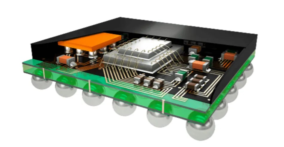
How SiP Technology Enhances Miniaturized Electronics
Miniaturization in electronics is driven by consumer demand for compact, high-performance devices that operate efficiently in constrained environments. SiP technology achieves this by:
Integrating multiple dies in a single package – Reducing PCB footprint and interconnect distances.
Optimizing power efficiency – Lowering power consumption through closer integration of components.
Enhancing signal integrity – Reducing parasitics and improving high-speed data transmission.
Supporting heterogeneous integration – Enabling different technologies (RF, logic, memory) to coexist.
By eliminating bulky PCB traces and external interconnects, SiP enhances overall system reliability while improving thermal performance and mechanical durability, making it ideal for wearable devices, IoT sensors and mobile applications.
Challenges and Innovations in SiP Manufacturing
Despite its advantages, SiP presents new manufacturing challenges, particularly in yield optimization, thermal management and high-precision interconnects. The complexity of stacking multiple dies, integrating passive components and ensuring high-speed connectivity requires advanced metrology and inspection techniques to maintain production efficiency.
Erik Hosler remarks, “Modern society is built on CMOS technology, but as we push the boundaries of what these devices can do, we must innovate within the CMOS framework to continue driving performance, efficiency, and integration.” His insights underscore the importance of refining SiP fabrication techniques to meet the demands of next-generation compact electronics.
The Future of SiP Technology in Next-Generation Devices
As SiP packaging continues to evolve, it will drive advancements in:
5G and RF integration – Enabling compact, power-efficient connectivity modules.
AI-enabled wearables – Enhancing smartwatches, medical implants and biometric sensors.
Edge computing applications – Supporting real-time processing in ultra-compact devices.
By revolutionizing electronic miniaturization, SiP technology is enabling the next wave of innovation, ensuring that future devices become more powerful, efficient and compact without compromising performance.

